


SKU/Artículo: AMZ-B0FZH2BBHD
XUSILAOK
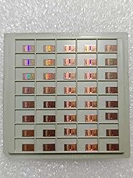
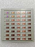
Non-Functional Silicon IC Die Wafer, Bare CPU Semiconductor Chip Sample with CMOS Lithography Patterns for Teaching, STEM Education, and Art Display (0.20" x 0.12" 1 Box /40 pcs)
Model:
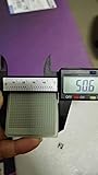
5 * 3Mm 1 box 40 pcs
Detalles del producto
Disponibilidad:
En stock
En stock
Peso con empaque:
0.23 kg
0.23 kg
Devolución:
No
No
Condición
Nuevo
Nuevo
Producto de:
Amazon
Amazon
Viaja desde
USA
USA
Sobre este producto
- This non-functional bare silicon die showcases genuine CMOS lithography and integrated circuit patterns created during semiconductor fabrication.It provides an up-close view of microchip architecture for education, research, and artistic purposes.Each die is precisely diced from a real wafer, polished, and safely packaged in an anti-static storage box.Perfect for students, engineers, and collectors who appreciate microelectronic design and silicon art.
AR$92.829
60% OFF
AR$37.132
IMPORT EASILY
By purchasing this product you can deduct VAT with your RUT number
AR$92.829
60% OFF
AR$37.132
con envío
Este producto viaja
de USA ![]() a tus manos en
a tus manos en
![]()
Conoce más detalles
IC Type: Semiconductor Each wafer fragment contains visible integrated circuit patterns for demonstration and display purposes only. Made from single-crystal silicon wafer material for authentic semiconductor teaching and research. Ideal for electronics courses, microfabrication demonstrations, and STEM student projects. Also suitable for art installations, photography props, and chip design exhibitions.
Compra protegida
Disfruta de una experiencia de compra segura y confiable
Tarjetas de Crédito y Débito
Visa
Mastercard
American Express
Pagos a través de PayPal
Compra procesada en dólares con dinero en cuenta o tarjetas internacionales.
Paypal
Pagos a través de MODO
Compra procesada en pesos desde la App de tu banco.
PayPal